- Deutsch
-
EnglishDeutschItaliaFrançais日本語한국의русскийSvenskaNederlandespañolPortuguêspolskiSuomiGaeilgeSlovenskáSlovenijaČeštinaMelayuMagyarországHrvatskaDanskromânescIndonesiaΕλλάδαБългарски езикAfrikaansIsiXhosaisiZululietuviųMaoriKongeriketМонголулсO'zbekTiếng ViệtहिंदीاردوKurdîCatalàBosnaEuskeraالعربيةفارسیCorsaChicheŵaעִבְרִיתLatviešuHausaБеларусьአማርኛRepublika e ShqipërisëEesti Vabariikíslenskaမြန်မာМакедонскиLëtzebuergeschსაქართველოCambodiaPilipinoAzərbaycanພາສາລາວবাংলা ভাষারپښتوmalaɡasʲКыргыз тилиAyitiҚазақшаSamoaසිංහලภาษาไทยУкраїнаKiswahiliCрпскиGalegoनेपालीSesothoТоҷикӣTürk diliગુજરાતીಕನ್ನಡkannaḍaमराठी
Comparing Thin Film and Thick Film Circuits
- 2024/10/15
- 22
Catalog
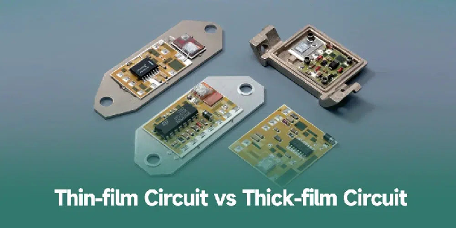
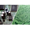
Understanding Thin Film Circuits
A thin film circuit is a network of devices and wires embedded in a thin layer of material, usually less than 100 nm thick. These circuits are made using advanced methods like thermal oxidation, chemical vapor deposition (CVD), physical vapor deposition (PVD), and epitaxial growth.
Thermal oxidation, creates a protective oxide layer, important for insulation and durability. CVD, uses chemical reactions to form precise, uniform films. PVD, transfers material to a surface, making ultra-thin and pure films. Epitaxial growth, forms a crystalline layer that is major for high-performance electronics.
These techniques are used in devices like micro electromechanical systems (MEMS), sensors, and advanced integrated circuits (ICs). Thin films are valuable in small, compact designs, such as portable electronics and wearables, where space is limited. As technology evolves, thin film circuits are likely to be used in even more tiny devices.
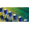
An Overview of Thick Film Circuits
A thick film circuit is an electronic circuit made by putting small parts on a surface using techniques like screen printing. The thickness of the film is usually a few microns to tens of microns, which makes it useful for many applications. The materials used include conductors, resistors, and insulators.
The thickness of the film is basic because it affects how well the circuit works.
Thick film circuits are easier and cheaper to make compared to other types. They can be produced in large quantities without needing complicated machines.
While making them is simple, designing them for specific uses can be more complex. These circuits can handle a lot of power, making them ideal for tough jobs in industries like manufacturing and automotive.
However, thick film circuits have some limits because they use standard materials and processes. This can restrict the types of components used. To get around this, you often combine thick film circuits with other technologies, like thin film or silicon integrated circuits (ICs), to improve their performance.
When deciding to use thick film circuits, you should consider how much power they need to handle and the cost of production.
Between Thin Film vs Thick Film Circuits
Film Thickness
The main difference between thin and thick film circuits is their thickness. Thick film circuits have a film that is usually thicker than 10μm, making them strong enough for high-power applications. This thickness allows them to handle larger currents and voltages without breaking down, which is great for power electronics. On the other hand, thin film circuits are typically less than 1μm thick. They are designed for precise electronic applications, balancing durability and accuracy in their design.
Manufacturing Process
The ways these circuits are made also differ outstandingly. Thick film circuits are created using a screen-printing method, where conductive, resistive, and insulating pastes are layered onto materials like ceramic. This method is simple and cost-effective, making it suitable for mass production. In contrast, thin film circuits require advanced techniques like vacuum evaporation and magnetron sputtering. These processes are done in clean room environments, where any tiny particles could affect the film’s quality and performance.
Applications
The unique properties of thick and thin film circuits lead to different applications. Thick film circuits are ideal for high-voltage, high-current, and high-power uses, making them useful in power electronics, automotive sensors, and industrial controls due to their strength and reliability. Thin film circuits, however, are used where precision and high integration are needed. They work well in environments that face high temperatures and corrosion, making them suitable for aerospace, military, and medical devices. Although thin film circuits can be more expensive, their performance in specialized applications often justifies the cost.
Verwandter Blog
-
Verständnis des C1815 -Transistors: Pinouts, Schaltungssymbole, Anwendungsschaltungen
2023/12/20
Welche Art von Röhre ist der C1815?C1815 Triode PinoutC1815 ModellzeichnungC1815 -ParameterC1815 EigenschaftenAnwendung von C1815 Der C1815 -Transist... -
Ein Überblick über TTL- und CMOS -ICs und wie Sie zwischen ihnen wählen

2024/04/13
In diesem Artikel werfen wir einen detaillierten Blick auf zwei wichtige elektronische Technologien, komplementäre Metaloxid-Halbleiter (CMOS) und Tr... -
Netzteilspannung Abkürzung: VCC VDD VEE VSS GND
2024/06/6
Im modernen elektronischen Schaltungsdesign, Verständnis der Abkürzungen der Stromversorgungsspannung (wie VCC, VDD, VEE, VSS, GND).Diese Abkürzung... -
LR44 -Batterien: LR44 -Batterieäquivalente und LR44 -Batterieersatz
2024/01/24
In einem sich schnell entwickelnden technologischen Gebiet, in dem die Größe der elektronischen Geräte weiter schrumpfen und dennoch alltäglicher ... -
Verschiedene Arten von Sicherungen und Anwendungen

2024/04/18
Sicherungen sind wesentliche Komponenten in modernen elektrischen Systemen und fungieren als entscheidende Beschützer vor Überstrom.Sie arbeiten, in... -
Beschreiben Sie kurz die Spezifikationen, Verpackungen, das Arbeitsprinzip, die Vorteile und die Umweltauswirkungen von Lithium-Ionen-Batterien
2024/03/20
Seit der Einführung von wiederaufladbaren Blei-Säure-Batterien im Jahr 1859 wurden sie allmählich in den Gewebe des technologischen Fortschritts ei... -
Leitfaden zu Buck-, Boost- und Buck-Boost-Konverter
2023/12/21
Was ist ein Buck -Konverter?Wie funktioniert ein Buck Converter?Was ist ein Boost -Konverter?Wie funktioniert ein Boost -Konverter?Was ist ein Auftrie... -
Grundkenntnisse über Sicherungen: Merkmale, Arbeitsprinzipien, Typen und wie man richtig auswählt
2024/04/10
Sicherungen schützen Schaltungen vor Schäden aufgrund von Überlastung oder Kurzstrecken.Dieses einfache, aber geniale Gerät basiert auf einem leic... -
Transistor (BJT und MOSFET) Arbeitsprinzipien
2023/12/20
Arbeitsprinzip des bipolaren Junction -Transistors (BJT)Auswahl der KomponentenwerteWie wählen Sie einen Transistor?Arbeitsprinzip von MOSFETWie scha... -
Beherrschen analoge und digitale Schaltungen: Ein Anfängerführer
2023/12/20
Definition und Eigenschaften von analogen Schaltungen und digitalen SchaltungenDer Unterschied zwischen analogen Schaltungen und digitalen Schaltungen... -
Transistor umfassender Leitfaden
2023/12/20
1. Was ist ein Transistor?2. Wie funktioniert ein Transistor?3. Vorteile von Transistoren4. Arten von Transistoren5.faq 1. Was ist ein Transistor? Ein... -
Eine vollständige Liste von Testmethoden für verschiedene Transistoren
2023/12/20
Der Transistor wurde von John Bardeen, William Shockley und Walter Brattain erfunden.Es handelt sich um ein Kollektor-, Emitter- und Basis-Drei-termin... -
Grunde elektronische Grundkomponenten verstehen - Widerstände, Kondensatoren, Dioden, Transistoren, Induktoren und digitale Logik -Tore
2024/04/13
Elektronische Komponenten sind der Eckpfeiler des Bauens und der Optimierung elektronischer Schaltkreise.Von gewöhnlichen Haushaltsgeräten bis hin z...